


Hongo Campus
Graduate SchoolGraduate School of Engineering - Electrical Engineering and Information Systems, (※)
DepartmentDepartment of Electrical and Electronic Engineering
Nano Physics & Device Technology Field
Nanostructural physics
Electronic materials/Electric materials
Electron device/Electronic equipment
Applied materials
Quantum Computing
Semiconductor
Condensed Matter Physics
Crystal engineering
Semiconductor Process Technology
New electronic materials / devices, spintronics, quantum science and technology
We are conducting research on new materials, hetero structures, nano structures, and devices, aiming to create new electronics using electronic spin functions and quantum phenomena. We are working on a wide range of themes, from basic research based on intellectual curiosity to research with an engineering application.
Research field 1
Study of new electronics - spintronics and quantum science and technology using spin degrees of freedom and quantum effects
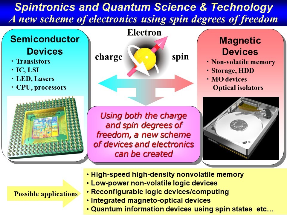
New electronics using electron spin degrees of freedom -- Spintronics, Quantum Science & Technology:
We are conducting basic research on new electronic materials and devices for their future applications to electronic, optical, and magnetic (spin) devices, as well as their hybrid devices. Specifically, (1) we perform epitaxial growth of nano-scale ultrathin films, artificial nanostructures, and quantum heterostructures in which quantum mechanical effects appear, using various materials such as semiconductors, metals, semimetals, ferromagnetic materials, superconductors, and topological materials. (2) We design and create new materials at the atomic level that do not exist in nature, and study the materials science and physical properties of these new materials, and fabricate prototypes of devices to provide guidelines for future electronics applications. In particular, we are focusing on the creation of new materials in which electron spin and its order (magnetism) are prominent and their application to semiconductor electronics, so called "spintronics". Furthermore, we aim to control the quantum states, including spin states, and develop quantum science and technology.
Research field 2
Creation of new materials, heterostructures, nanostructures, and quantum materials that combine spin and semiconductor functions and their device applications
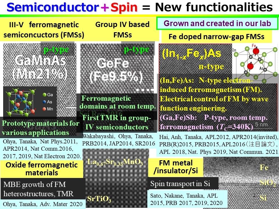
Creation of new materials, heterostructures, nanostructures, and quantum materials with both spin and semiconductor functions and their device applications:
By integrating spin functions in semiconductors, we create ferromagnetic semiconductors, various new materials, their thin films, heterostructures, and nanostructures, and study their new functionalities. Recently, we are also studying quantum materials and quantum science and technology. Many new materials are created by epitaxial growth techniques using several molecular beam epitaxy systems in our laboratory, controlling film thickness and structure at the atomic level. There are many materials and structures that can only be produced by our research in the world, and this is the source of the originality and strength of our research. We conduct research from the fundamental manufacturing process of crystal growth and material creation, and aim for innovation in materials science, electronics, information technology, and energy conservation technology.
Research field 3
Creation of a new device "spin transistor" using electron conduction and spin degrees of freedom
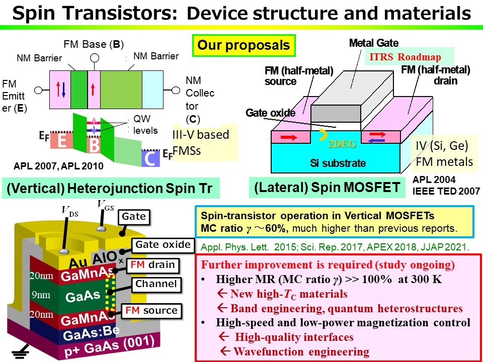
Creation of new devices "spin transistors" using electron transport and spin degrees of freedom:
Examples of spintronics devices are shown. The upper left figure shows a (vertical-type) heterojunction spin transistor using spin-dependent quantum level control, and the upper right figure shows a (lateral-type) Spin-MOSFET using spin-dependent conduction. Both of these devices are called "spin transistors" that we proposed. The common feature of these spin transistors is that they are three-terminal devices that can operate as transistors, and at the same time, the output characteristics can be changed in a non-volatile manner depending on the relative magnetization direction (parallel or anti-parallel magnetization) of the two ferromagnetic layers contained in the device. The output characteristics can be changed non-volatilely after the device is fabricated. By taking advantage of such features as variable output characteristics after fabrication, these spin transistors can be used to design ultra-high-density nonvolatile memory, reconfigurable logic circuits (logic circuits whose functions can be non-volatilely rewritten many times after fabrication), and flexible information processing systems such as neuromorphic computing and artificial intelligence. If memory and logic can be made nonvolatile and placed in semiconductor integrated circuits, it is expected to make a significant contribution to the low-power consumption of information processing systems.