


YOKOTA Tomoyuki Associate Professor
Hongo Campus
Graduate SchoolGraduate School of Engineering - Electrical Engineering and Information Systems
DepartmentDepartment of Electrical and Electronic Engineering
Nano Physics & Device Technology Field
Biomedical engineering/Biomaterial science and engineering
Nanostructural physics
Thin film/Surface and interfacial physical properties
Electronic materials/Electric materials
Electron device/Electronic equipment
Semiconductor
Photonics
Semiconductor Process Technology
Wearable Devices
Biosensing/imaging
Healthcare Technology
Organic electronics for flexible sensor application
Our group develop the soft electronics by organic materials. Our focus is Device Physics, Development of new process, Application.
Research field 1
Ultra-flexible Organic photonic devices
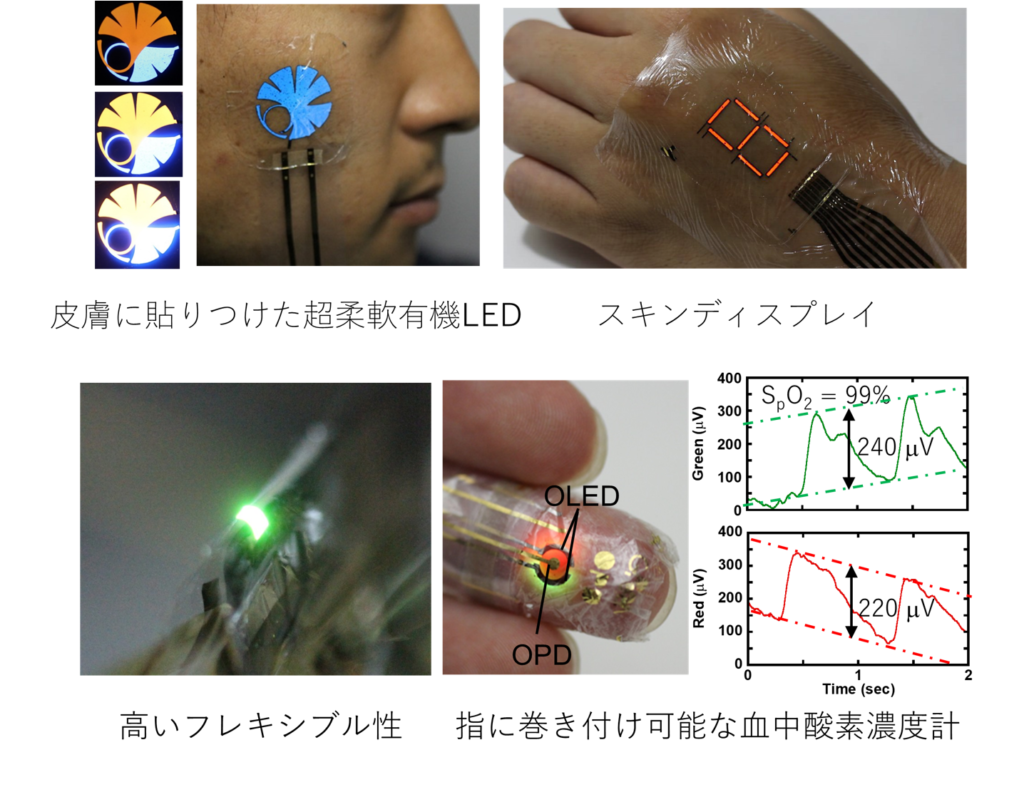
Flexible electronics have many advatages that conventional electronics do not have, such as high flexibility and light weight. It is vey important to reduce the thickness of the substrate to take full advantage of these features. Our laboratory has focused on organic photonic devices, and has developed technologies to form these devices on ultra-thin substrates.We have realized organic light emitting diode and photodetector on ultra-thin film substrates as thin as 1 µm by using low-damage and solution processes. We are working on improving the characteristics and stability of these devices for sensor applications.
Research field 2
Sensor application of the ultra-flexible organic photonic devices
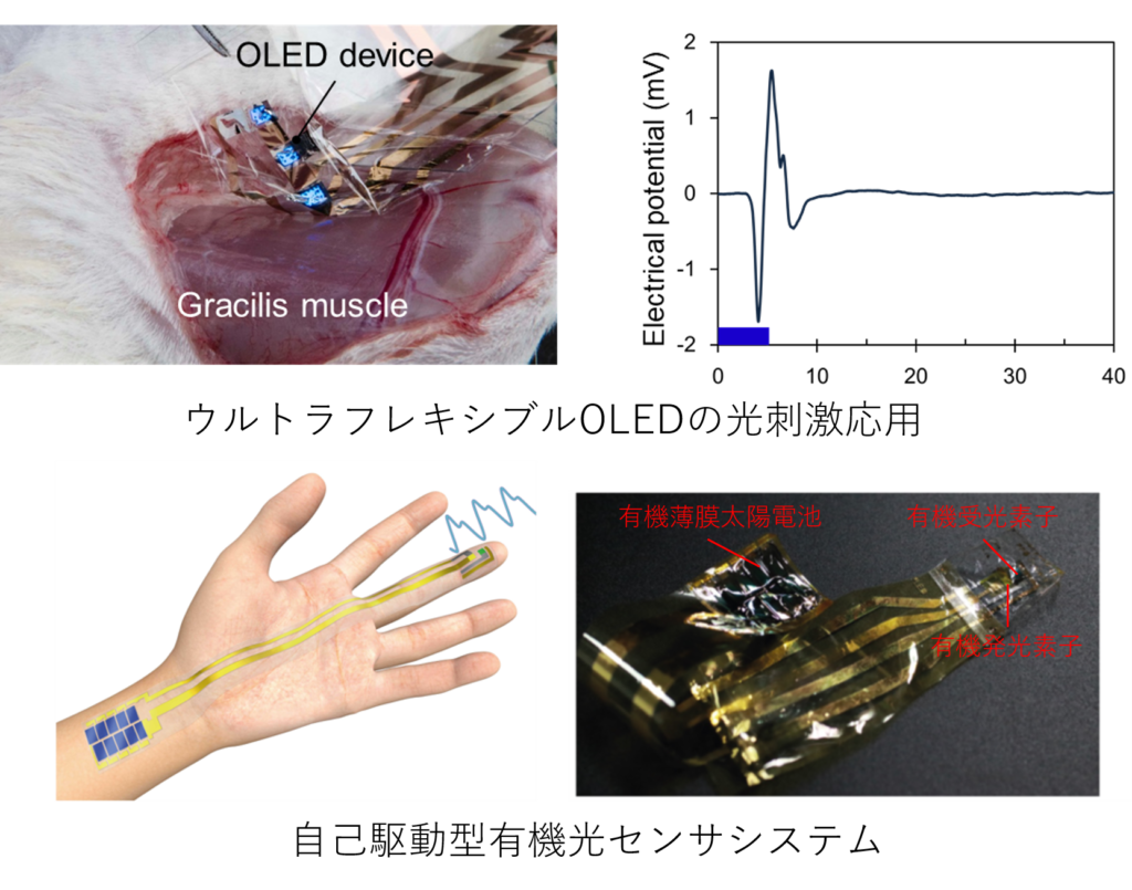
Since light can measure inside information from outside of the body, optical-imaging-based approaches, such as X-rays, are widely used for disease diagnosis in hospitals. Our group is developing the sensor application using our ultra-flexible organic photonic devices. Especially, we added the functionality to the device by integrating organic light emitting diode, organic photodetector and organic transistor on the same substrate. Until now, we have realized an ultra-thin light source for optical stimulation and a pulse wave sensor that can be operated by sunlight.
Research field 3
Sheet type image sensor
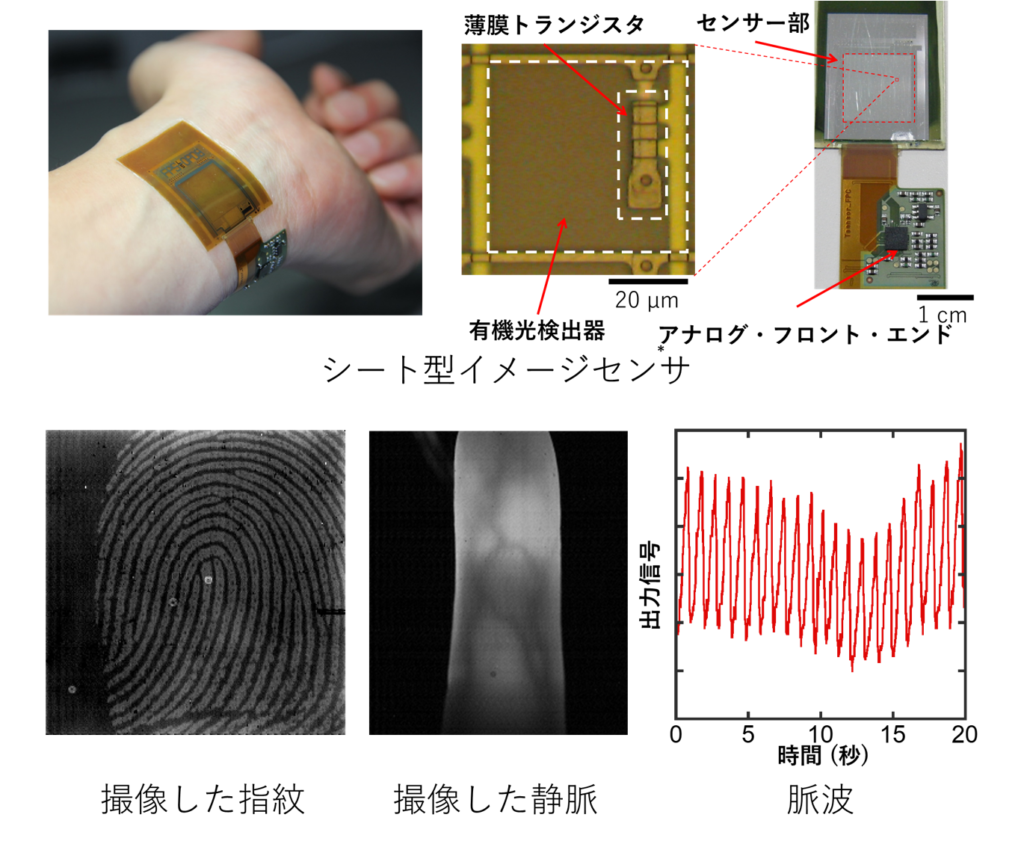
One of the important applications of photonic device is image sensors. We collaborated with the company to develop a flexible sheet type image sensor for biometric authentication. Up to now, we have developed a sheet type sensor that can take an image of fingerprints and veins by integrating low-temperature polysilicon thin-film transistors and an organic photodetector. Furthermore, this image sensor can measure pulse wave signal and take an image of the fingerprint simultaneously.
Research field 4
Printable and high sensitive temperature sensor
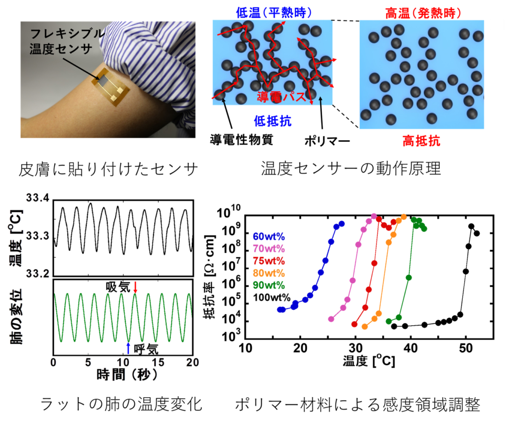
Our laboratory is also working on the development of materials with new functionality. In particular, we are working on the development of printable sensor materials. Until now, we have succeeded in developing a temperature-sensitive sensor material that shows a large resistance change near body temperature. This sensor material has been realized by synthesizing a novel polymer material with a controllable melting point and dispersing conductive particles in it.
Research field 5
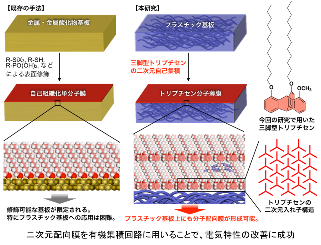
A two dimentional high orederd film that can be formed on the polymer substrate
It is important to control the surface state of the substrate for forming the thin film layer. that serves as the substrate. In general, the surface energy and other properties of oxides and metals has been controlled by forming a self-assembled monolayer on the substrate, using chemical bonding. On the other hand, in organic materials such as polymers, it has been difficult to form oriented films due to weak bonding. In collaboration with Prof. Fukushima's group at Tokyo Institute of Technology, our laboratory has developed a new technology to form a few molecules of alignment film on plastic substrate without chemical bonding by using tripodal triptycene molecules. This technology is expected to enhance the functionality of organic electronics.